Go to content

Research

Many of the optical and electronic properties of solids are caused by extremely fast dynamics of electrons on the femtosecond (1 fs = 10-15 s) time scale. Our main interest is to trace ultrafast processes, while resolving the impact of interfaces, strong light-matter coupling, or local structural changes on the nanometer (1 nm = 10-9 m) length scale. We are developing new methods to effectively capture nano-femto-dynamics, allowing us to record nanoscopic slow-motion pictures.

Ultrafast nano-optical imaging

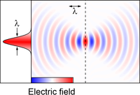
Abbe diffraction limit
Due to its wave-like nature, light can only be focused to focal spot sizes on the order of the wavelength λ with conventional optics. In the mid-infrared (MIR) spectral range, for example, this is not sufficient for imaging nanostructures due to the long wavelength (λ~10 µm).
Near-field microscopy
One way to circumvent this limit is to use the evanescent near fields at the apex of a sharp metallic tip. In near-field microscopy [1,2], the attainable resolution is mostly set by the radius of curvature of the apex. This approach has allowed for sidestepping the diffraction limit by orders of magnitude. The light scattered from the tip-sample system (red arrows) is analyzed. This allows for retrieving the optical properties of the sample, described by a dielectric function ε, with nanoscale precision (see inset) [3].
Subcycle resolution and pump-probe scheme
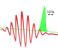
Combining the above approach with ultrafast lasers grants simultaneous temporal resolution on the order of a few femtoseconds. Upon excitation with an optical pump pulse (green), electron-hole pairs are generated in semiconductor samples. A subsequent probe pulse (red) interrogates the out-of-equilibrium dynamics in a stroboscopic fashion [4].
In the MIR, not only the intensity envelope of the scattered light pulses is accessible, but even the electric field itself. Using electro-optic sampling – an oscilloscope for light – the scattered waveform (red) may be resolved in absolute amplitude and phase with sub-optical cycle (= subcycle) precision [5].

Van der Waals materials

Van der Waals materials

Van der Waals quantum materials represent a versatile material platform with applicatons in energy harvesting, sensing, and nanophotonics.
Transition metal dichalcogenides
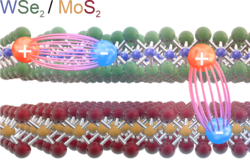
The atomically thin nature of monolayers of transition metal dichalcogenides, such as MoS2 or WSe2, renders these two-dimensional sheets extremely susceptible to their environment. In addition, the weak dielectric screening leads to strong Coulomb attraction between electrons (blue) and holes (red). Bound states, so-called excitons, with binding energies of hundreds of meV emerge. These excitons dominate the optical response of monolayer transition metal dichalcogenides [6].

Their properties can be tuned by interlayer coupling [7], the twist angle [8], or the dielectric environment [9]. On ultrafast time scales, excitons may be spatially separated across a van der Waals interface, which affects their life time and binding energy substantially [10].


Moiré superlattices

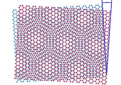
When stacking two monolayers on top of each other with a twist angle or a lattice mismatch, the lattices interfere with each other. The emerging, larger-scale superlattice is typically referred to as a moiré pattern. Electrons experience this periodic modulation of the atomic registry as a potential landscape, which has several consequences. For instance, excitons may get trapped in the moiré potential. Furthermore, the electron-electron interaction can be strongly enhanced, leading to pronounced correlations that induce phase transitions. We want to resolve these and related exciting phenomena directly in space and time.


Hybrid light-matter modes

Hybrid light-matter modes

Polaritons are comprised of light and matter excitations, such as phonons and plasmons. These modes are often strongly localized to interfaces and feature wavevectors that exceed those of free-space electromagnetic radiation by up to two orders of magnitude. This strong confinement and the resulting enhancement of electromagnetic fields renders polaritons promising for nanophotonic circuits and applications in sensing and subdiffractional optics.
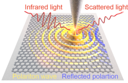
Nano-optical imaging of
light-matter modes

The evanescent fields at the apex of the near-field tip can bridge the momentum mismatch and launch polariton waves. This approach has widely been used to image interference patterns of polariton waves in van der Waals crystals [11].

Thin slabs of van der Waals crystals may also act as waveguides [12,13] for infrared radiation. In this case, the polaritons propagate through the volume and are not confined to the surface.

Controlling polariton dispersion
For future applications, a high level of control over the propagation of polaritons is desirable. Femtosecond photo-excitation has facilitated the ultrafast switching of polariton waves [4]. We aim to further introduce a subcycle detection of the wavefronts. For additional degrees of control, we want to rely on exotic material properties similar to the twist-tunable elliptical/hyperbolic dispersion in MoO3.


References (for further details, see Publications)

  1. Chen et al., Adv. Mater. 31, 1804774 (2019)
  2. Mooshammer et al., ACS Photonics 7, 344–351 (2020)
  3. Mooshammer et al., Nano Letters 18, 7515–7523 (2018)
  4. Huber, F.M. et al., Nature Nanotechnology 12, 207–211 (2017)
  5. Plankl, F.M. et al., Nature Photonics 15, 594–600 (2021)
  6. Wang, Chernikov et al., Rev. Mod. Phys. 90, 021001 (2018)
  7. Kunstmann, F.M. et al., Nature Physics 14, 801–805 (2018)
  8. Merkl, F.M. et al., Nature Communications 11, 2167 (2020)
  9. Zhang, F.M. et al., Nature Communications 13, 542 (2022)
  10. Merkl, F.M. et al., Nature Materials 18, 691–696 (2019)
  11. Basov, Fogler, García de Abajo, Science 354, aag1992 (2016)
    Low et al., Nature Materials 16, 182–194 (2017)
  12. Mooshammer et al., ACS Photonics 9, 443–451 (2022)
  13. Mooshammer et al., ACS Nano 18, 4118–4130 (2024)

Subcycle Nano-Optics Group


Address:

Regensburg Center for Ultrafast Nanoscopy
University of Regensburg
Universitätsstraße 31
93053 Regensburg
Germany